PL-Analysis
Determining Material Properties under Lasing Conditions from Low Excitation Luminescence
Here
is an example of a closed-loop wafer growth to photo luminescence
and gain-measurement of processed sample.
The idea is explained in more detail in Refs.[15]
and [16].
The structure is an MBE grown electrically pumped p-i-n doped
multi quantum-well structure. The active region consists nominally
of three 5 nm wide In0.2Ga0.8As quantum wells between GaAs barriers.
In the absence of external pump voltage and pump carriers the
doping profile has been calculated to result in an internal electric
field across the active region of 34 kV/cm.

STEP 1: Nominal Spontaneous Emission (PL)

In the first step the spontaneous emission (PL) for several densities in the low
density regime is calculated using the semiconductor luminescence equations
for the nominal structural parameters
(layer widths and compositions). Here, as in typical PL experiments,
optical pumping is assumed, i.e. the dopant related electric fields
are present. The spectra are only homogenbeously broadenend (due
to electron-electron and electron-phonon scattering), there is
no inhomogeneous broadening.
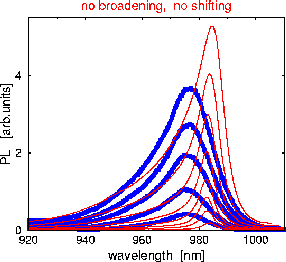
Comparing the results to experimental spectra shows that
the theoretical spectra are 6 nm off the experimental peak positions.
This shift can here be either due to an actual Indium concentration
of 19% instead of the nominal 20%, or a well width which is 4.5
nm instead of the nominal 5 nm.
The above
picture shows the theoretical PL spectra in the absence
of inhomogeneous broadening and for the nominal structural parameters (red lines) and the
measured PL spectra (blue lines). The theoretical results are
for carrier densities of 0.1, 0.17, 0.23, 0.3, 0.4, 0.53, 0.68
and 0.86x10¹²/cm². The experimental results are for optical pump
powers of 12, 16, 18, 21 and 24mW.

STEP 2: Comparison to the Experimental PL

A
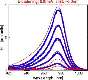
match to the experimental spectra can only be found for an inhomogeneous
broadening of 9.8 meV (Gaussian broadening; half width at 1/e
amplitude) and when associating the rather uncertain experimental
pump powers with the theoretical densities as shown in the picture.
This broadening corresponds to well width fluctuations of rather
implausibly high 0.5 nm, and/or a more probable fluctuation of
the Indium-composition of 1%.
The
above picture shows the theoretical PL spectra for the
determined material parameters (19% Indium) and inhomogeneous
broadening (9.8 meV) (red lines) and the measured PL spectra as already shown under Step 1
(blue lines). The theoretical results are for carrier densities
of 0.1, 0.17, 0.23, 0.3, 0.4, 0.53, 0.68 and 0.86x10¹²/cm².

STEP 3: Actual Gain and Absorption

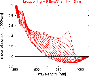
Using the actual material parameters and inhomogeneous broadening
determined in Step 2 the absorption and gain spectra for the device
under lasing conditions are calculated. The doping related electric
fields across the active region are absent when using electrical
pumping.
The above picture shows resulting gain/absorption spectra
for densities of between 0.5 and 4.5x10¹²/cm² with density steps
of 0.25x10¹²/cm² between neighbouring spectra.

STEP 4: Testing the Resulting Gain

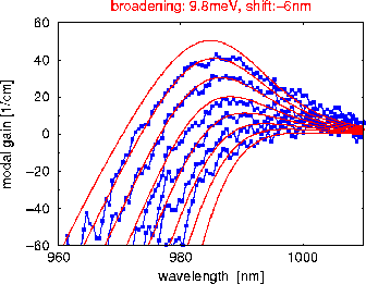
For this device the gain spectra have actually been measured in
order to test the approach. The theoretical spectra are for the
actual material parameters and inhomogeneous broadening as determined
from the PL-analysis. No additional spectral shifting, broadening
or amplitude-scaling has been used to modify the theoretical results.
The above picture shows theoretical spectra for densities
of 1.0, 1.125, 1.25, 1.375, 1.5, 1.625, 1.75 and 1.875x10¹²/cm²
(red lines). The experimental pump currents are 6.0, 6.5, 7.0,
7.5, 8.3, and 9.0 mA. The experimental spectra have been measured
using the Hakki-Paoli method.


